- 您现在的位置:买卖IC网 > Sheet目录479 > MMFT5P03HDT1 (ON Semiconductor)MOSFET P-CH 30V 3.7A SOT223
�� �
�
�MMFT5P03HD�
�12�
�QT�
�24�
�1000�
�V� DD� =� 15� V�
�I� D� =� 4� A�
�8�
�V� DS�
�V� GS�
�16�
�V� GS� =� 10� V�
�T� J� =� 25� °� C�
�100�
�t� d(off)�
�t� f�
�4�
�Q1�
�Q2�
�8�
�t� r�
�I� D� =� 4� A�
�Q3�
�T� J� =� 25� °� C�
�t� d(on)�
�0�
�0�
�4�
�8�
�12�
�16�
�20�
�0�
�10�
�1�
�10�
�100�
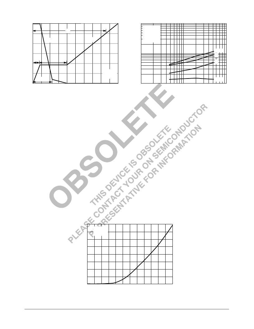
�Q� G� ,� TOTAL� GATE� CHARGE� (nC)�
�Figure� 8.� Gate� ?� To� ?� Source� and� Drain� ?� To� ?� Source�
�Voltage� versus� Total� Charge�
�R� G� ,� GATE� RESISTANCE� (OHMS)�
�Figure� 9.� Resistive� Switching� Time�
�Variation� versus� Gate� Resistance�
�DRAIN� ?� TO� ?� SOURCE� DIODE� CHARACTERISTICS�
�The� switching� characteristics� of� a� MOSFET� body� diode�
�are� very� important� in� systems� using� it� as� a� freewheeling� or�
�commutating� diode.� Of� particular� interest� are� the� reverse�
�recovery� characteristics� which� play� a� major� role� in�
�determining� switching� losses,� radiated� noise,� EMI� and� RFI.�
�System� switching� losses� are� largely� due� to� the� nature� of�
�the� body� diode� itself.� The� body� diode� is� a� minority� carrier�
�device,� therefore� it� has� a� finite� reverse� recovery� time,� t� rr� ,� due�
�to� the� storage� of� minority� carrier� charge,� Q� RR� ,� as� shown� in�
�the� typical� reverse� recovery� wave� form� of� Figure� 11.� It� is� this�
�stored� charge� that,� when� cleared� from� the� diode,� passes�
�through� a� potential� and� defines� an� energy� loss.� Obviously,�
�repeatedly� forcing� the� diode� through� reverse� recovery�
�further� increases� switching� losses.� Therefore,� one� would�
�like� a� diode� with� short� t� rr� and� low� Q� RR� specifications� to�
�minimize� these� losses.�
�The� abruptness� of� diode� reverse� recovery� effects� the�
�amount� of� radiated� noise,� voltage� spikes,� and� current�
�ringing.� The� mechanisms� at� work� are� finite� irremovable�
�circuit� parasitic� inductances� and� capacitances� acted� upon� by�
�4�
�V� GS� =� 0� V�
�T� J� =� 25� °� C�
�3�
�2�
�1�
�high� di/dts.� The� diode’s� negative� di/dt� during� t� a� is� directly�
�controlled� by� the� device� clearing� the� stored� charge.�
�However,� the� positive� di/dt� during� t� b� is� an� uncontrollable�
�diode� characteristic� and� is� usually� the� culprit� that� induces�
�current� ringing.� Therefore,� when� comparing� diodes,� the�
�ratio� of� t� b� /t� a� serves� as� a� good� indicator� of� recovery�
�abruptness� and� thus� gives� a� comparative� estimate� of�
�probable� noise� generated.� A� ratio� of� 1� is� considered� ideal� and�
�values� less� than� 0.5� are� considered� snappy.�
�Compared� to� ON� Semiconductor� standard� cell� density�
�low� voltage� MOSFETs,� high� cell� density� MOSFET� diodes�
�are� faster� (shorter� t� rr� ),� have� less� stored� charge� and� a� softer�
�reverse� recovery� characteristic.� The� softness� advantage� of�
�the� high� cell� density� diode� means� they� can� be� forced� through�
�reverse� recovery� at� a� higher� di/dt� than� a� standard� cell�
�MOSFET� diode� without� increasing� the� current� ringing� or� the�
�noise� generated.� In� addition,� power� dissipation� incurred�
�from� switching� the� diode� will� be� less� due� to� the� shorter�
�recovery� time� and� lower� switching� losses.�
�0�
�0.5�
�0.6�
�0.7�
�0.8�
�0.9�
�1�
�1.1�
�V� SD� ,� SOURCE?TO?DRAIN� VOLTAGE� (VOLTS)�
�Figure� 10.� Diode� Forward� Voltage� versus� Current�
�http://onsemi.com�
�6�
�发布紧急采购,3分钟左右您将得到回复。
相关PDF资料
MMFT960T1
MOSFET N-CH 60V 300MA SOT223
MMG3002NT1
IC AMP RF GP 3600MHZ 5.2V SOT-89
MMG3006NT1
TRANS GPA 33DBM 16-QFN
MMG3007NT1
IC AMP RF GP 6000MHZ 5V SOT-89
MMG3H21NT1
TRANS HBT 20.5DBM 19.3DB SOT-89
MMH3111NT1
TRANS GAAS HFET SOT-89
MML20211HT1
IC LNA 2GHZ 21P1DB 8DFN
MMS-1A-V2 0
SENSOR MICRO MACHINED SMD
相关代理商/技术参数
MMFT5P03HDT3
制造商:MOTOROLA 制造商全称:Motorola, Inc 功能描述:TMOS P-CHANNEL FIELD FEECT TRANSISTOR
MMFT6N03HD
制造商:MOTOROLA 制造商全称:Motorola, Inc 功能描述:TMOS POWER 6.0 AMPERES 30 VOLTS
MMFT960T1
功能描述:MOSFET 60V 300mA N-Channel RoHS:否 制造商:STMicroelectronics 晶体管极性:N-Channel 汲极/源极击穿电压:650 V 闸/源击穿电压:25 V 漏极连续电流:130 A 电阻汲极/源极 RDS(导通):0.014 Ohms 配置:Single 最大工作温度: 安装风格:Through Hole 封装 / 箱体:Max247 封装:Tube
MMFT960T1_06
制造商:ONSEMI 制造商全称:ON Semiconductor 功能描述:Power MOSFET 300 mA, 60 Volts N−Channel SOT−223
MMFT960T1G
功能描述:MOSFET 60V 300mA N-Channel RoHS:否 制造商:STMicroelectronics 晶体管极性:N-Channel 汲极/源极击穿电压:650 V 闸/源击穿电压:25 V 漏极连续电流:130 A 电阻汲极/源极 RDS(导通):0.014 Ohms 配置:Single 最大工作温度: 安装风格:Through Hole 封装 / 箱体:Max247 封装:Tube
MMFTN123
制造商:Diotec Semiconductor 功能描述:
MMFTN138
制造商:Diotec 功能描述:Bulk
MMFTN170
制造商:Diotec Semiconductor 功能描述: